Visit Google Scholar page for up-to-date citation information.
Nari Hong, Boil Kim, Jaewon Lee, Han Kyung Choe, Kyong Hwan Jin*, and Hongki Kang*
Machine learning-based high-frequency neuronal spike reconstruction from low-frequency and low-sampling-rate recordings, Nature Communications, 2024.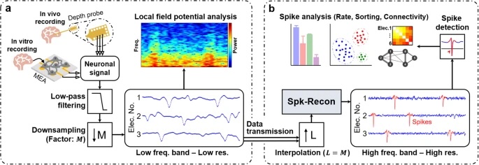
Donghoon Lee, Jungha Lee, Minhye Shin, Duhee Kim, Junhee Lee, Murali Bissannagari, Woongki Hong, Jae Eun Jang, Jaewon Jang*, and Hongki Kang*
Sangwoo Hwang, Yujin Hwang, Duhee Kim, Junhee Lee, Han Kyoung Choe, Junghyup Lee, Hongki Kang, Jaeha Kung*
Seunghun Baik, Heejae Jeong, Geuntae Park, Hongki Kang, Jae Eun Jang, Hyuk-Jun Kwon
Reducing specific contact resistivity for n-type germanium using laser activation process and nano-island formation, Applied Surface Science, 2023.
Hyeongtae Lim, Hyeokjin Kwon, Hongki Kang, Jae Eun Jang & Hyuk-Jun Kwon
Minkyung Sim, Jeonggyun Jang, Kwonsik Shin, Dongsu Kim, Joonghyun Kim, Hyuk-Jun Kwon, Hongki Kang, and Jae Eun Jang
Duhee Kim, Nari Hong, Woongki Hong, Junhee Lee, Murali Bissannagari, Youngjae Cho, Hyuk-Jun Kwon, Jae Eun Jang, and Hongki Kang*
Inkjet-Printed Polyelectrolyte Seed Layer-Based, Customizable, Transparent, Ultrathin Gold Electrodes and Facile Implementation of Photothermal Effect, ACS APPLIED MATERIALS & INTERFACES, 2023.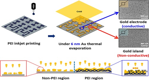
MEDIA
- DGIST
- 전자신문: 환자 맞춤형 투명 금 전극 제작기술 개발
- 헤럴드경제
Chong-Myeong Song, Dongsu Kim, Hyungtae Lim, Hongki Kang, Jae Eun Jang, and Hyuk-Jun Kwon*
Unlocking performance potential of two-dimensional SnS2 transistors with solution-processed high-k Y:HfO2 film and semimetal bismuth contact., APPLIED SURFACE SCIENCE, 2023.
Hongki Kang*, Yoonkey Nam
The Effect of Electrostatic Force between the Nanoparticles and the Substrate on the Uniform Assembly of Inkjet-Printed Nanoparticles, JOURNAL OF FLEXIBLE AND PRINTED ELECTRONICS,1(1) 2022.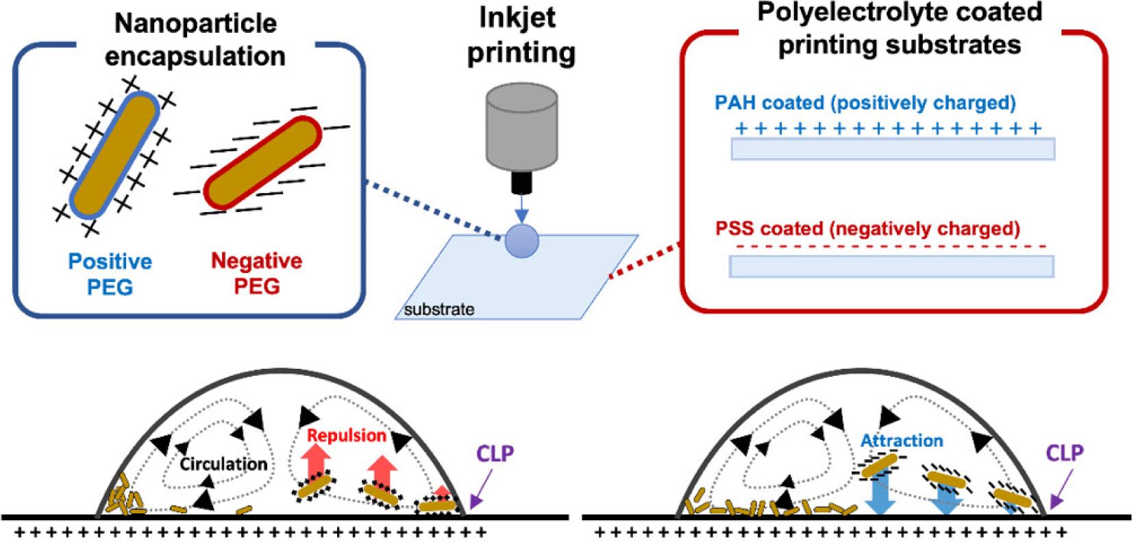
Bongho Jang, Junhee Lee, Hongki Kang, Jaewon Jang, Hyuk-Jun Kwon*
Schottky Barrier Modulation of Bottom Contact SnO2 Thin-Film Transistors via Chloride-Based Combustion Synthesis, JOURNAL OF MATERIALS SCIENCE & TECHNOLOGY, 2022.
Yujin Hwang†, Jungha Lee†, Su Jin Heo, Nari Hong, Junhee Lee, Jae Eun Jang, Hongki Kang*
a-IGZO thin-film transistors with transparent ultrathin Al/Ag bilayer source and drain for active neural interfaces, MATERIALS SCIENCE IN SEMICONDUCTOR PROCESSING, 2023.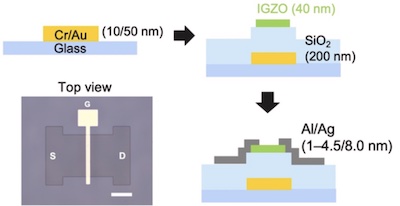
Junhee Lee†, Seongkwon Hwang†, Nari Hong†, Jeonghun Kwak, Jae Eun Jang, Seungjun Chung*, Hongki Kang*
High temporal resolution transparent thermoelectric temperature sensors for photothermal effect sensing, MATERIALS HORIZONS, 2022.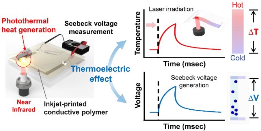
MEDIA
- DGIST, “빛에 의한 온도 변화를 정밀하게 측정하는 생체 친화적 투명 온도센서 기술 개발”
- 전자신문
- 헤럴드경제
Heejae Jeong, Y.S. Kim, Seunghun Baik, Hongki Kang, Jae Eun Jang, and Hyuk-Jun Kwon*
Kwonsik Shin, Eunmin Choi, Minkyung Sim, Minsoo Kang, Ji-Woong Choi, SeungNam Cha, Hyuk-Jun Kwon, Hongki Kang, Jae Eun Jang*
Fundamental Insights into the Electrical Signals of a Piezoelectric Sensor in a Sliding Condition, Nano Energy, 2022.
Min Soo Kang, Hyun Woo Jang, Min Kyung Sim, Kwonsik Shin, Dong Su Kim, Hongki Kang, Hyuk-Jun Kwon, and Jae Eun Jang*
Detecting temperature of small object using hybrid tactile sensor array and multi-parameter extraction analysis, SENSORS AND ACTUATORS A: PHYSICAL, 2022.
Junhee Lee, Nari Hong, Woongki Hong, Duhee Kim, Yujin Hwang, Jaewon Jang, Hongki Kang*
Semi-transparent, micrometer resolution p-NiO/n-ZnO heterojunction diode temperature sensors with ultrathin metal anode, ADVANCED MATERIALS TECHNOLOGIES, 2022.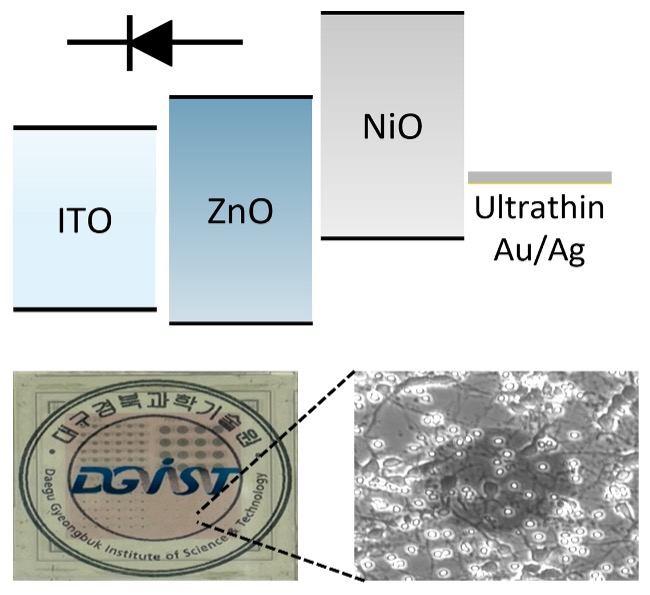
Woongki Hong, Jee Woong Lee, Duhee Kim, Yujin Hwang, Junhee Lee, Junil Kim, Nari Hong, Hyuk-Jun Kwon, Jae Eun Jang, Anna Rostedt Punga, Hongki Kang*
Ultrathin Gold Microelectrode Array using Polyelectrolyte Multilayers for Flexible and Transparent Electro-Optical Neural Interfaces, ADVANCED FUNCTIONAL MATERIALS, 32, 2106493, 2022.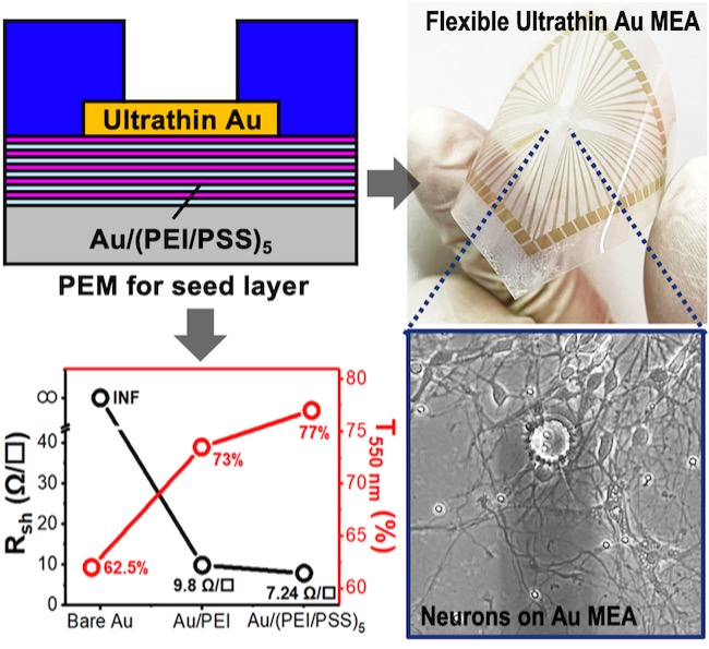
MEDIA
- DGIST, “얇은 금으로 만들어 유연하면서도 투명한 뇌신경 전극 개발”
- 한국경제
- 헤럴드경제
Kyoungdu Kim, Woongki Hong, Changmin Lee, Won-Yong Lee, Do Won Kim, Hyeon Joong Kim, Hyuk-Jun Kwon, Hongki Kang* and Jaewon Jang*
Sol-Gel-Processed Amorphous-Phase ZrO2 Based Resistive Random Access Memory, MATERIALS RESEARCH EXPRESS, 8 116301, 2021.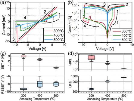
Woongki Hong, Junhee Lee, Duhee Kim, Yujin Hwang, Hyuk-Jun Kwon, Jae Eun Jang and Hongki Kang*
Computational Thermal Analysis of the Photothermal Effect of Thermoplasmonic Optical Fiber for Localized Neural Stimulation In Vivo, ELECTRONICS,10(2), 118, 2021.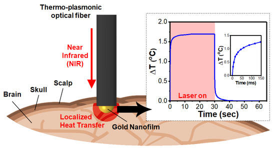
Seunghun Baik, Dong-Jae Kwon, Hongki Kang, Jae Eun Jang, Jaewon Jang, Y.S. Kim, Hyuk-Jun Kwon
Conformal and ultra shallow junction formation achieved using a pulsed-laser annealing process integrated with a modified plasma assisted doping method, IEEE ACCESS, 8, 172166 - 172174, 2020. 
Hongki Kang, Woongki Hong, Yujin An, Sangjin Yoo, Hyuk-Jun Kwon, Yoonkey Nam
Thermoplasmonic Optical Fiber for Localized Neural Stimulation, ACS NANO, 14, 9, 11406–11419, 2020.
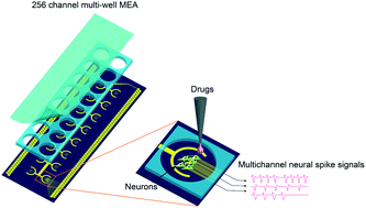
Daejeong Kim, Hongki Kang and Yoonkey Nam
Compact 256-channel multi-well microelectrode array system for in vitro neuropharmacology test, LAB ON A CHIP, 20, 3410-3422, 2020.
Su Jin Heo, Seunguk Kim, Goeun Pyo, Jae Hoon Yang, Jeonghee Shin, Hyuk-Jun Kwon, Hongki Kang, Gae Hwang Lee, and Jae Eun Jang
Color Thin-Film Transistors Employing Periodic Nanohole Structures, ACS APPLIED ELECTRONIC MATERIALS,2, 8, 2489–2497, 2020.
Bongho Jang, Hongki Kang, Won-Yong Lee, Jin-Hyuk Bae, In-Man Kang, Kwangeun Kim, Hyuk-Jun Kwon, and Jaewon Jang
Enhancement mode Flexible SnO2 Thin Film Transistors via a UV/Ozone Assisted Sol-Gel Approach, IEEE ACCESS, 8, 123013-123018, 2020. 
Changmin Lee, Won-Yong Lee, Hyunjae Lee, Seunghyun Ha, Jin-Hyuk Bae, In-Man Kang, Hongki Kang, Kwangeun Kim, Jaewon Jang
Sol-gel processed yttrium-doped SnO2 thin film transistors, ELECTRONICS,9(2), 254, 2020.
Hongki Kang, Jee Woong Lee, and Yoonkey Nam
Inkjet-Printed Multi-Wavelength Thermo-Plasmonic Images for Anti-Counterfeiting Applications, ACS APPLIED MATERIALS & INTERFACES, 10, 7, 6764–6771, 2018.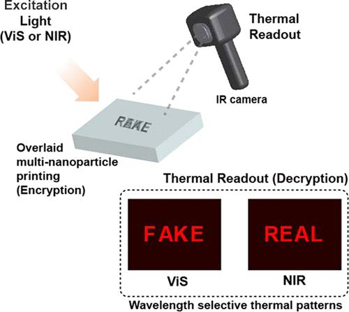
Jee Woong Lee‡, Hongki Kang‡, and Yoonkey Nam
Thermo-Plasmonic Gold Nanofilm for Simple and Mass-Producible Photothermal Neural Interfaces, NANOSCALE, 10, 9, 9226–9235, 2018.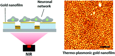
Hongki Kang, Gu-Haeng Lee, Hyunjun Jung, Jee Woong Lee and Yoonkey Nam
Inkjet-Printed Biofunctional Thermo-Plasmonic Interfaces for Patterned Neuromodulation, ACS NANO, 12, 2, 1128–1138, 2018.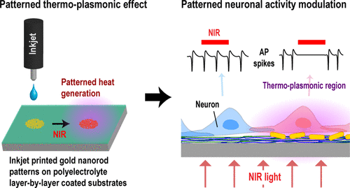
MEDIA
- Nature Index, “Printing personalized brain implants”
- 전자신문, “뇌질환 치료용 나노입자 프린팅 기술 개발”
- ScienceDaily, “Printed thermo-plasmonic heat pattern for neurological disorder treatment.”
Bongho Jang, Taegyun Kim, Sojeong Sojeong Lee, Won-yong Lee, Hongki Kang, Chan Seob Cho, Jaewon Jang
Hongki Kang, Jee-Yeon Kim, Yang-Kyu Choi, and Yoonkey Nam
Feasibility Study of Extended-gate Type Silicon Nanowire Field-Effect Transistor for Neural Recording, SENSORS, 17(4), 705, 2017.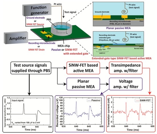
Hyunjun Jung, Hongki Kang, and Yoonkey Nam
Digital Micromirror based Near-infrared Illumination System for Plasmonic Photothermal Neuromodulation, BIOMEDICAL OPTICS EXPRESS, 8, 2866, 2017.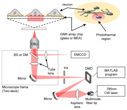
Gerd Grau, Jialiang Cen, Hongki Kang, Rungrot Kitsomboonloha, William Scheideler, and Vivek Subramanian
Vivek Subramanian, Jialiang Cen, Alejandro de la Fuente Vornbrock, Gerd Grau, Hongki Kang, Rungrot Kitsomboonloha, Daniel Soltman, and Huai-Yuan Tseng
Gerd Grau, Rungrot Kitsomboonloha, Hongki Kang, and Vivek Subramanian
High performance printed organic transistors using a novel scanned thermal annealing technology, ORGANIC ELECTRONICS, vol. 20, pp. 150–157, 2015.
Jaewon Jang, Hongki Kang, Himamshu C. Nallan Chakravarthula, and Vivek Subramanian
Fully inkjet-printed transparent oxide thin film transistors using a fugitive wettability switch, ADVANCED ELECTRONIC MATERIALS, vol. 1, no. 7, 2015.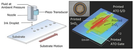
Rungrot Kitsomboonloha, Hongki Kang, Gerd Grau, William Scheideler, and Vivek Subramanian
MHz-Range Fully Printed High-Performance Thin-Film Transistors by Using High-Resolution Gravure-Printed Lines, ADVANCED ELECTRONIC MATERIALS, vol. 1, no. 12, 2015.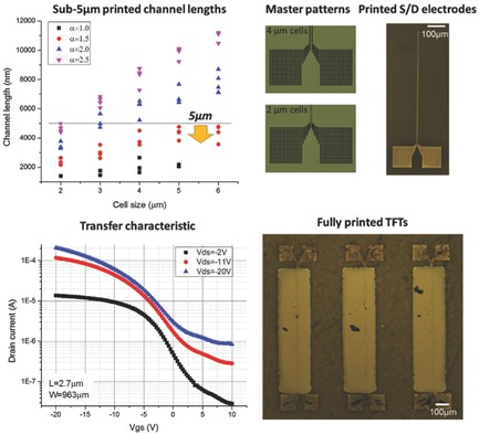
Hongki Kang, Rungrot Kitsomboonloha, Kurt Ulmer, Lisa Stecker, Gerd Grau, Jaewon Jang and Vivek Subramanian
Megahertz-class printed high mobility organic thin-film transistors and inverters on plastic using attoliter-scale high-speed gravure-printed sub-5 μm gate electrodes, ORGANIC ELECTRONICS, vol. 15, no. 12, pp. 3639–3647, Dec. 2014.
Gerd Grau, Rungrot Kitsomboonloha, Sarah L Swisher, Hongki Kang, Vivek Subramanian
Hyuk-Jun Kwon‡, Hongki Kang‡, Jaewon Jang, Sunkook Kim, and Costas P. Grigoropoulos
Hongki Kang, Rungrot Kitsomboonloha, Jaewon Jang, and Vivek Subramanian
High-performance printed transistors realized using femtoliter gravure-printed Sub-10μm metallic nanoparticle patterns and highly uniform polymer dielectric and semiconductor layers, ADVANCED MATERIALS, vol. 24, no. 22, pp. 3065–3069, 2012.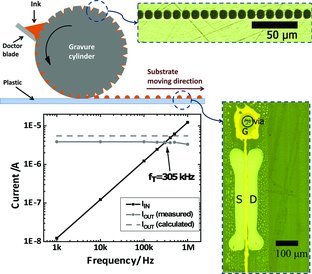
Jaewon Jang, Rungrot Kitsomboonloha, Sarah L. Swisher, Eung Seok Park, Hongki Kang, and Vivek Subramanian
Transparent High-Performance Thin Film Transistors from Solution-Processed SnO2/ZrO2 Gel-like Precursors, ADVANCED MATERIALS, vol. 25, no. 7, pp. 1042–1047, 2012.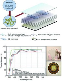
Alejandro de la Fuente Vornbrock, Donovan Sung, Hongki Kang, Rungrot Kitsomboonloha, and Vivek Subramanian
Dan Soltman, Ben Smith, Hongki Kang, S.J.S. Morris, and Vivek Subramanian
Methodology for inkjet printing partially wetting films, LANGMUIR, 26 (19), pp 15686-15693, 2010.
Hongki Kang, Dan Soltman, and Vivek Subramanian
Hydrostatic Optimization of Inkjet-Printed Films, LANGMUIR, 26(13), 11568-11573, 2010.
Nari Hong, Boil Kim, Jaewon Lee, Han Kyung Choe, Kyong Hwan Jin*, and Hongki Kang*
Machine learning-based high-frequency neuronal spike reconstruction from low-frequency and low-sampling-rate recordings, Nature Communications, 2024.
Donghoon Lee, Jungha Lee, Minhye Shin, Duhee Kim, Junhee Lee, Murali Bissannagari, Woongki Hong, Jae Eun Jang, Jaewon Jang*, and Hongki Kang*
Sangwoo Hwang, Yujin Hwang, Duhee Kim, Junhee Lee, Han Kyoung Choe, Junghyup Lee, Hongki Kang, Jaeha Kung*
Seunghun Baik, Heejae Jeong, Geuntae Park, Hongki Kang, Jae Eun Jang, Hyuk-Jun Kwon
Reducing specific contact resistivity for n-type germanium using laser activation process and nano-island formation, Applied Surface Science, 2023.
Hyeongtae Lim, Hyeokjin Kwon, Hongki Kang, Jae Eun Jang & Hyuk-Jun Kwon
Minkyung Sim, Jeonggyun Jang, Kwonsik Shin, Dongsu Kim, Joonghyun Kim, Hyuk-Jun Kwon, Hongki Kang, and Jae Eun Jang
Duhee Kim, Nari Hong, Woongki Hong, Junhee Lee, Murali Bissannagari, Youngjae Cho, Hyuk-Jun Kwon, Jae Eun Jang, and Hongki Kang*
Inkjet-Printed Polyelectrolyte Seed Layer-Based, Customizable, Transparent, Ultrathin Gold Electrodes and Facile Implementation of Photothermal Effect, ACS APPLIED MATERIALS & INTERFACES, 2023.
MEDIA
- DGIST
- 전자신문: 환자 맞춤형 투명 금 전극 제작기술 개발
- 헤럴드경제
Chong-Myeong Song, Dongsu Kim, Hyungtae Lim, Hongki Kang, Jae Eun Jang, and Hyuk-Jun Kwon*
Unlocking performance potential of two-dimensional SnS2 transistors with solution-processed high-k Y:HfO2 film and semimetal bismuth contact., APPLIED SURFACE SCIENCE, 2023.
Bongho Jang, Junhee Lee, Hongki Kang, Jaewon Jang, Hyuk-Jun Kwon*
Schottky Barrier Modulation of Bottom Contact SnO2 Thin-Film Transistors via Chloride-Based Combustion Synthesis, JOURNAL OF MATERIALS SCIENCE & TECHNOLOGY, 2022.
Yujin Hwang†, Jungha Lee†, Su Jin Heo, Nari Hong, Junhee Lee, Jae Eun Jang, Hongki Kang*
a-IGZO thin-film transistors with transparent ultrathin Al/Ag bilayer source and drain for active neural interfaces, MATERIALS SCIENCE IN SEMICONDUCTOR PROCESSING, 2023.
Hongki Kang*, Yoonkey Nam
The Effect of Electrostatic Force between the Nanoparticles and the Substrate on the Uniform Assembly of Inkjet-Printed Nanoparticles, JOURNAL OF FLEXIBLE AND PRINTED ELECTRONICS,1(1) 2022.
Junhee Lee†, Seongkwon Hwang†, Nari Hong†, Jeonghun Kwak, Jae Eun Jang, Seungjun Chung*, Hongki Kang*
High temporal resolution transparent thermoelectric temperature sensors for photothermal effect sensing, MATERIALS HORIZONS, 2022.
MEDIA
- DGIST, “빛에 의한 온도 변화를 정밀하게 측정하는 생체 친화적 투명 온도센서 기술 개발”
- 전자신문
- 헤럴드경제
Heejae Jeong, Y.S. Kim, Seunghun Baik, Hongki Kang, Jae Eun Jang, and Hyuk-Jun Kwon*
Kwonsik Shin, Eunmin Choi, Minkyung Sim, Minsoo Kang, Ji-Woong Choi, SeungNam Cha, Hyuk-Jun Kwon, Hongki Kang, Jae Eun Jang*
Fundamental Insights into the Electrical Signals of a Piezoelectric Sensor in a Sliding Condition, Nano Energy, 2022.
Min Soo Kang, Hyun Woo Jang, Min Kyung Sim, Kwonsik Shin, Dong Su Kim, Hongki Kang, Hyuk-Jun Kwon, and Jae Eun Jang*
Detecting temperature of small object using hybrid tactile sensor array and multi-parameter extraction analysis, SENSORS AND ACTUATORS A: PHYSICAL, 2022.
Junhee Lee, Nari Hong, Woongki Hong, Duhee Kim, Yujin Hwang, Jaewon Jang, Hongki Kang*
Semi-transparent, micrometer resolution p-NiO/n-ZnO heterojunction diode temperature sensors with ultrathin metal anode, ADVANCED MATERIALS TECHNOLOGIES, 2022.
Woongki Hong, Jee Woong Lee, Duhee Kim, Yujin Hwang, Junhee Lee, Junil Kim, Nari Hong, Hyuk-Jun Kwon, Jae Eun Jang, Anna Rostedt Punga, Hongki Kang*
Ultrathin Gold Microelectrode Array using Polyelectrolyte Multilayers for Flexible and Transparent Electro-Optical Neural Interfaces, ADVANCED FUNCTIONAL MATERIALS, 32, 2106493, 2022.
MEDIA
- DGIST, “얇은 금으로 만들어 유연하면서도 투명한 뇌신경 전극 개발”
- 한국경제
- 헤럴드경제
Kyoungdu Kim, Woongki Hong, Changmin Lee, Won-Yong Lee, Do Won Kim, Hyeon Joong Kim, Hyuk-Jun Kwon, Hongki Kang* and Jaewon Jang*
Sol-Gel-Processed Amorphous-Phase ZrO2 Based Resistive Random Access Memory, MATERIALS RESEARCH EXPRESS, 8 116301, 2021.
Woongki Hong, Junhee Lee, Duhee Kim, Yujin Hwang, Hyuk-Jun Kwon, Jae Eun Jang and Hongki Kang*
Computational Thermal Analysis of the Photothermal Effect of Thermoplasmonic Optical Fiber for Localized Neural Stimulation In Vivo, ELECTRONICS,10(2), 118, 2021.
Seunghun Baik, Dong-Jae Kwon, Hongki Kang, Jae Eun Jang, Jaewon Jang, Y.S. Kim, Hyuk-Jun Kwon
Conformal and ultra shallow junction formation achieved using a pulsed-laser annealing process integrated with a modified plasma assisted doping method, IEEE ACCESS, 8, 172166 - 172174, 2020.
Hongki Kang, Woongki Hong, Yujin An, Sangjin Yoo, Hyuk-Jun Kwon, Yoonkey Nam
Thermoplasmonic Optical Fiber for Localized Neural Stimulation, ACS NANO, 14, 9, 11406–11419, 2020.
Daejeong Kim, Hongki Kang and Yoonkey Nam
Compact 256-channel multi-well microelectrode array system for in vitro neuropharmacology test, LAB ON A CHIP, 20, 3410-3422, 2020.
Su Jin Heo, Seunguk Kim, Goeun Pyo, Jae Hoon Yang, Jeonghee Shin, Hyuk-Jun Kwon, Hongki Kang, Gae Hwang Lee, and Jae Eun Jang
Color Thin-Film Transistors Employing Periodic Nanohole Structures, ACS APPLIED ELECTRONIC MATERIALS,2, 8, 2489–2497, 2020.
Bongho Jang, Hongki Kang, Won-Yong Lee, Jin-Hyuk Bae, In-Man Kang, Kwangeun Kim, Hyuk-Jun Kwon, and Jaewon Jang
Enhancement mode Flexible SnO2 Thin Film Transistors via a UV/Ozone Assisted Sol-Gel Approach, IEEE ACCESS, 8, 123013-123018, 2020.
Changmin Lee, Won-Yong Lee, Hyunjae Lee, Seunghyun Ha, Jin-Hyuk Bae, In-Man Kang, Hongki Kang, Kwangeun Kim, Jaewon Jang
Sol-gel processed yttrium-doped SnO2 thin film transistors, ELECTRONICS,9(2), 254, 2020.
Hongki Kang, Jee Woong Lee, and Yoonkey Nam
Inkjet-Printed Multi-Wavelength Thermo-Plasmonic Images for Anti-Counterfeiting Applications, ACS APPLIED MATERIALS & INTERFACES, 10, 7, 6764–6771, 2018.
Jee Woong Lee‡, Hongki Kang‡, and Yoonkey Nam
Thermo-Plasmonic Gold Nanofilm for Simple and Mass-Producible Photothermal Neural Interfaces, NANOSCALE, 10, 9, 9226–9235, 2018.
Hongki Kang, Gu-Haeng Lee, Hyunjun Jung, Jee Woong Lee and Yoonkey Nam
Inkjet-Printed Biofunctional Thermo-Plasmonic Interfaces for Patterned Neuromodulation, ACS NANO, 12, 2, 1128–1138, 2018.
MEDIA
- Nature Index, “Printing personalized brain implants”
- 전자신문, “뇌질환 치료용 나노입자 프린팅 기술 개발”
- ScienceDaily, “Printed thermo-plasmonic heat pattern for neurological disorder treatment.”
Bongho Jang, Taegyun Kim, Sojeong Sojeong Lee, Won-yong Lee, Hongki Kang, Chan Seob Cho, Jaewon Jang
Hongki Kang, Jee-Yeon Kim, Yang-Kyu Choi, and Yoonkey Nam
Feasibility Study of Extended-gate Type Silicon Nanowire Field-Effect Transistor for Neural Recording, SENSORS, 17(4), 705, 2017.
Hyunjun Jung, Hongki Kang, and Yoonkey Nam
Digital Micromirror based Near-infrared Illumination System for Plasmonic Photothermal Neuromodulation, BIOMEDICAL OPTICS EXPRESS, 8, 2866, 2017.
Gerd Grau, Jialiang Cen, Hongki Kang, Rungrot Kitsomboonloha, William Scheideler, and Vivek Subramanian
Vivek Subramanian, Jialiang Cen, Alejandro de la Fuente Vornbrock, Gerd Grau, Hongki Kang, Rungrot Kitsomboonloha, Daniel Soltman, and Huai-Yuan Tseng
Gerd Grau, Rungrot Kitsomboonloha, Hongki Kang, and Vivek Subramanian
High performance printed organic transistors using a novel scanned thermal annealing technology, ORGANIC ELECTRONICS, vol. 20, pp. 150–157, 2015.
Jaewon Jang, Hongki Kang, Himamshu C. Nallan Chakravarthula, and Vivek Subramanian
Fully inkjet-printed transparent oxide thin film transistors using a fugitive wettability switch, ADVANCED ELECTRONIC MATERIALS, vol. 1, no. 7, 2015.
Rungrot Kitsomboonloha, Hongki Kang, Gerd Grau, William Scheideler, and Vivek Subramanian
MHz-Range Fully Printed High-Performance Thin-Film Transistors by Using High-Resolution Gravure-Printed Lines, ADVANCED ELECTRONIC MATERIALS, vol. 1, no. 12, 2015.
Hongki Kang, Rungrot Kitsomboonloha, Kurt Ulmer, Lisa Stecker, Gerd Grau, Jaewon Jang and Vivek Subramanian
Megahertz-class printed high mobility organic thin-film transistors and inverters on plastic using attoliter-scale high-speed gravure-printed sub-5 μm gate electrodes, ORGANIC ELECTRONICS, vol. 15, no. 12, pp. 3639–3647, Dec. 2014.
Gerd Grau, Rungrot Kitsomboonloha, Sarah L Swisher, Hongki Kang, Vivek Subramanian
Hyuk-Jun Kwon‡, Hongki Kang‡, Jaewon Jang, Sunkook Kim, and Costas P. Grigoropoulos
Hongki Kang, Rungrot Kitsomboonloha, Jaewon Jang, and Vivek Subramanian
High-performance printed transistors realized using femtoliter gravure-printed Sub-10μm metallic nanoparticle patterns and highly uniform polymer dielectric and semiconductor layers, ADVANCED MATERIALS, vol. 24, no. 22, pp. 3065–3069, 2012.
Jaewon Jang, Rungrot Kitsomboonloha, Sarah L. Swisher, Eung Seok Park, Hongki Kang, and Vivek Subramanian
Transparent High-Performance Thin Film Transistors from Solution-Processed SnO2/ZrO2 Gel-like Precursors, ADVANCED MATERIALS, vol. 25, no. 7, pp. 1042–1047, 2012.
Alejandro de la Fuente Vornbrock, Donovan Sung, Hongki Kang, Rungrot Kitsomboonloha, and Vivek Subramanian
Dan Soltman, Ben Smith, Hongki Kang, S.J.S. Morris, and Vivek Subramanian
Methodology for inkjet printing partially wetting films, LANGMUIR, 26 (19), pp 15686-15693, 2010.
Hongki Kang, Dan Soltman, and Vivek Subramanian
Hydrostatic Optimization of Inkjet-Printed Films, LANGMUIR, 26(13), 11568-11573, 2010.